8-Bit Programmable Computer - Technical Documentation#
1. Project Overview#
This project documents the design and implementation of a fully functional 8-bit breadboard computer with microcode-based control architecture. The system integrates arithmetic operations, memory storage, programmable instruction execution, and real-time visual feedback via LEDs and 7-segment displays. Built entirely from discrete TTL logic circuits, this computer demonstrates fundamental digital design principles including bus arbitration, finite state machines, and microcoded instruction sets.
Key Features:
- Von Neumann Architecture: Unified memory for instructions and data
- 8-bit Data Bus: Central communication pathway for all modules
- Microcoded Control: EEPROM-based instruction microstepping (8 steps per instruction)
- Full ALU: 8-bit addition and subtraction with 2's complement arithmetic
- Programmable RAM: 16 bytes of user-accessible memory
- Real-time Feedback: 97 LEDs showing bus state and control signals
- Manual Control Modes: Astable, monostable, and bistable clock options
2. Technical Specifications#
| Specification | Value |
|---|---|
| Architecture | 8-Bit Bus-Oriented Von Neumann |
| Data Bus Width | 8 bits [7:0] |
| Address Bus Width | 4 bits [3:0] |
| RAM Capacity | 16 Bytes (256 bits) |
| RAM Address Range | 0x0 to 0xF |
| Instruction Format | 8 bits: [7:4] opcode, [3:0] operand |
| Instruction Set Size | 10 instructions (7 functional, 3 unused) |
| Microinstruction Width | 16 bits (control signals) |
| Microinstruction Steps | 8 per instruction (0–7) |
| Microinstruction ROM Address | 7 bits: {Opcode[3:0], Step[2:0]} |
| Microinstruction ROM Size | 2732 EEPROM (4K × 8 bits) |
| ALU Operations | 2: Addition (A+B), Subtraction (A−B) |
| ALU Bit Width | 8 bits |
| ALU Components | Two 74LS283 (4-bit adders, cascaded) |
| Clock Frequency Range | 0.571 Hz to 400 Hz (astable mode) |
| Clock Generation | NE555 Timers (4 × astable/monostable/bistable) |
| Power Supply | 5V DC (regulated) |
| Total IC Count | 61 integrated circuits |
| Total Component Count | 262 discrete components |
| Display Type | 4 × 7-segment LED displays |
| Display Driver ROM | 2732 EEPROM (1024 bytes) |
| LED Feedback | 97 LEDs (8 data bus + 16 control signal + 73 digit display) |
3. System Architecture#
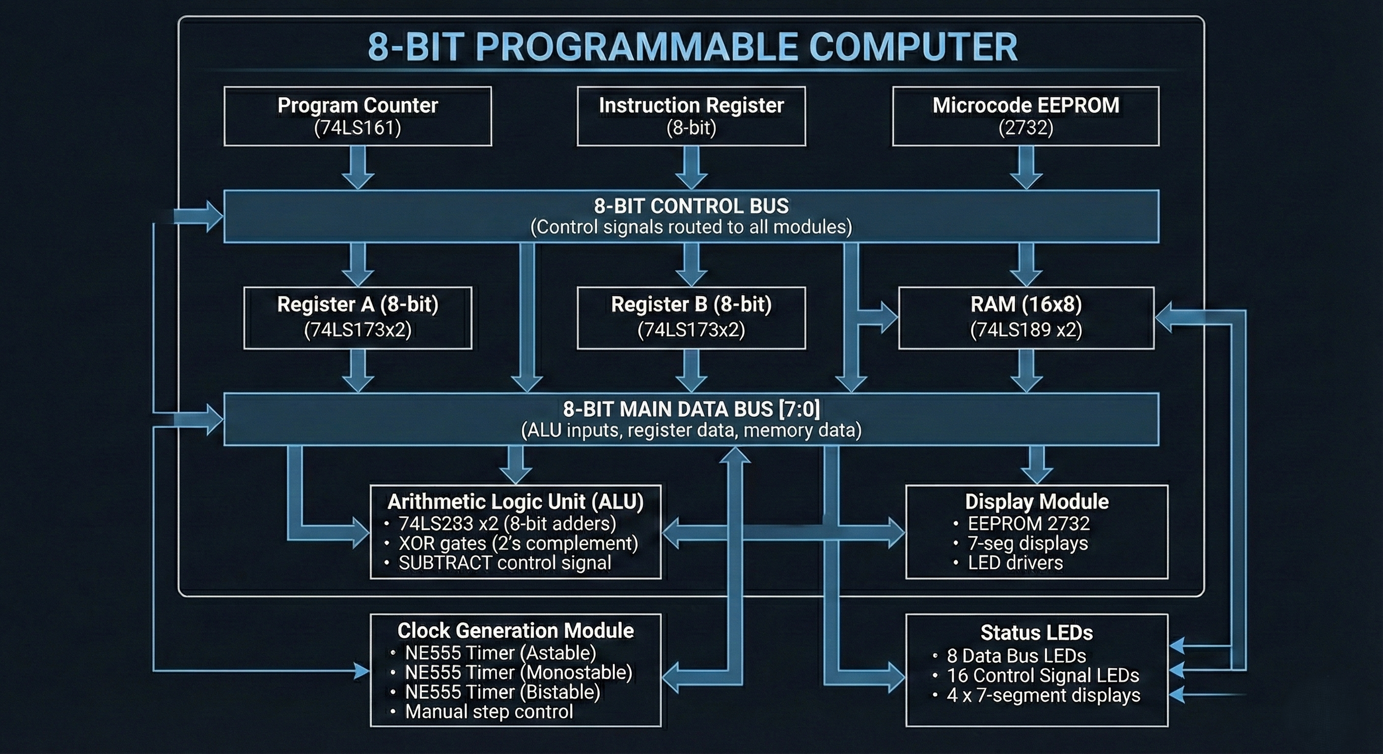
3.1 Overall Block Diagram
3.2 Data Bus Organization
The 8-bit data bus [7:0] is the central communication pathway:
| Bus Bits | Users | Bit Width | Purpose |
|---|---|---|---|
| [7:0] | Reg A, Reg B, ALU, RAM, IR input | 8 bits | Full-width data transfer |
| [7:0] | Display input, LED indicators | 8 bits | Display and feedback |
| [3:0] | PC output, MAR input, IR output | 4 bits | Address and operand transfer |
Bus Control Rules (enforced by microcode):
- Only ONE module drives the bus at any time (tristate logic)
- RAM_OUT and RAM_IN are never simultaneous
- All data transfers occur within a single clock cycle
4. Hardware Modules (Detailed)#
4.1 Program Counter (PC)
Component: 74LS161 (4-bit Synchronous Binary Counter)
- Function: Tracks current instruction address (0x0 to 0xF)
- Inputs:
- Clock signal from clock module
- PC_COUNTER_EN (increment enable)
- PC_COUNTER_JUMP (load new address)
- Outputs:
- 4-bit address to bus [3:0] via PC_COUNTER_OUT
- Increments on every clock pulse (when PC_COUNTER_EN=1)
- Loads new address when PC_COUNTER_JUMP=1
Operational Modes:
PC_COUNTER_EN=1, PC_COUNTER_JUMP=0 → PC ← PC + 1 (normal increment)
PC_COUNTER_EN=0, PC_COUNTER_JUMP=1 → PC ← Bus[3:0] (jump)
PC_COUNTER_EN=1, PC_COUNTER_JUMP=1 → PC ← Bus[3:0] (jump overwrites increment)
PC_COUNTER_EN=0, PC_COUNTER_JUMP=0 → PC unchanged (hold)
4.2 Instruction Register (IR) & Operand Decoder
Instruction Register:
- Component: 8-bit parallel-load register
- Input: 8-bit instruction from bus via INSTRUCT_IN
- Output:
- Upper nibble [7:4] → Opcode (used as part of microcode ROM address)
- Lower nibble [3:0] → Operand (output to bus via INSTRUCT_OUT)
Instruction Format:
Bit:     7 6 5 4 | 3 2 1 0
        ┌────────┬────────┐
Data:   │   Opcode    │ Operand     │
        └────────┴────────┘
Example: 0 0 1 0 | 1 1 1 1  (ADD instruction with operand 0xF)
4.3 Step Counter
Component: 74LS161 (4-bit Synchronous Counter)
- Function: Generates micro-steps 0–7 within each instruction cycle
- Clock: Same clock as system
- Reset: Automatically resets to 0 at the start of each new instruction
- Output: 3 bits [2:0] used as part of microcode ROM address
Fetch-Decode-Execute Cycle:
Instruction Fetch (Steps 0–1):
  Step 0: PC → MAR (address setup)
  Step 1: RAM[PC] → IR, PC ← PC+1 (fetch and increment)

Instruction Decode & Execute (Steps 2–7):
  Step 2: Operand address setup
  Step 3: Data fetch/compute phase 1
  Step 4: Data fetch/compute phase 2
  Steps 5–7: Unused (remain 0 for most instructions)
4.4 Microcode ROM (Control EEPROM)
Component: 2732 EEPROM (4K × 8 bits)
- Address Input: 7 bits = {Opcode[3:0], Step[2:0]}
- Data Output: 8 bits (lower 8 of 16 control signals)
- Function: Maps instruction-step pairs to control signals
Address Space:
Opcode × 8 Steps = 16 instructions × 8 steps = 128 entries

Entry format: EEEE_SSS
  EEEE = Instruction opcode [3:0]
  SSS = Micro-step [2:0]

Example:
  Instruction LDA (0001) + Step 3 → ROM address = 0b0001_011 = 0x0B
  ROM[0x0B] contains control signals for "Load A from RAM"
16-bit Control Signal Mapping:
Bit 0:  pc_counter_out    (PC output to bus)
Bit 1:  mem_in            (MAR input from bus)
Bit 2:  ram_out           (RAM output to bus)
Bit 3:  ram_in            (RAM input from bus)
Bit 4:  instruct_in       (IR input from bus)
Bit 5:  instruct_out      (IR operand output to bus)
Bit 6:  load_a_in         (Register A input)
Bit 7:  load_a_out        (Register A output)
Bit 8:  load_b_in         (Register B input)
Bit 9:  load_b_out        (Register B output)
Bit 10: sum_out           (ALU output to bus)
Bit 11: subtract          (ALU operation: 0=add, 1=subtract)
Bit 12: pc_counter_en     (PC increment enable)
Bit 13: pc_counter_jump   (PC load from bus)
Bit 14: display_d_in      (Display input)
Bit 15: halt              (System halt signal)
4.5 CPU Registers (A and B)
Component: 74LS173 (4-bit registers, 2 instances per 8-bit register)
Register A (Primary Accumulator):
- Size: 8 bits (using two 74LS173 chips)
- Input: 8-bit data from bus via LOAD_A_IN
- Output: 8-bit data to bus via LOAD_A_OUT
- Function:
- Stores intermediate results
- Primary ALU input
- Display output (when OUT instruction executes)
- Target for all arithmetic results
Register B (Temporary Register):
- Size: 8 bits (using two 74LS173 chips)
- Input: 8-bit data from bus via LOAD_B_IN
- Output: 8-bit data to bus via LOAD_B_OUT
- Function:
- Stores operand for arithmetic operations
- Secondary ALU input
- Intermediate storage during multi-step operations
Register Load Logic:
If LOAD_A_IN = 1: A ← Bus[7:0]
If LOAD_A_OUT = 1: Bus[7:0] ← A (drives bus)
If LOAD_B_IN = 1: B ← Bus[7:0]
If LOAD_B_OUT = 1: Bus[7:0] ← B (drives bus)
4.6 Arithmetic Logic Unit (ALU)
Components: Two 74LS283 (4-bit binary adders, cascaded for 8-bit)
Inputs:
- First operand: Register A [7:0]
- Second operand: Register B [7:0]
- Control signal: SUBTRACT (0 = add, 1 = subtract)
Operation:
When SUBTRACT = 0:
  Result = A + B (standard 8-bit binary addition)

When SUBTRACT = 1:
  Result = A - B (using 2's complement)
  Computation: A + (~B) + 1 (via XOR gates creating ~B)
Output:
- 8-bit result placed on bus via SUM_OUT control signal
- No internal storage; output is combinational
ALU Truth Table (Example Values):
A      | B      | SUBTRACT | Result | Operation
-------|--------|----------|--------|----------
0x05   | 0x03   | 0        | 0x08   | 5 + 3 = 8
0x08   | 0x03   | 1        | 0x05   | 8 - 3 = 5
0xFF   | 0x01   | 0        | 0x00   | 255 + 1 = 0 (overflow)
0x00   | 0x01   | 1        | 0xFF   | 0 - 1 = 255 (borrow, 2's complement)
4.7 Random Access Memory (RAM)
Component: 74LS189 (64-bit Static RAM, 2 instances for 16×8 bits)
Specifications:
- Capacity: 16 words × 8 bits = 128 bits total
- Address Space: 0x0 to 0xF (4-bit addressing)
- Access Time: <50 ns (read)
- Setup Time: Asynchronous read, synchronous write
Interface:
- Address Input: 4 bits [3:0] from bus via MEM_IN
- Data Input: 8 bits [7:0] from bus via RAM_IN
- Data Output: 8 bits [7:0] to bus via RAM_OUT
- Read/Write Control: Enforced by microcode (RAM_OUT and RAM_IN never simultaneous)
Memory Map (Default):
Address | Usage
--------|---------------------------
0x0–0x3 | Instruction area
0x4–0xD | Additional instruction space
0xE–0xF | Data storage (constants/variables)
Example Program Layout:
0x0: 0x1E  LDA 0xE    (Load 5 from address 0xE into A)
0x1: 0x2F  ADD 0xF    (Add value at 0xF to A)
0x2: 0xE0  OUT        (Display A)
0x3: 0xF0  HLT        (Halt)
...
0xE: 0x05  (Data: value 5)
0xF: 0x03  (Data: value 3)
4.8 Clock Generation Module
Components: Four NE555 Precision Timers
Mode 1: Astable (Free-running oscillator)
Frequency Range: 0.571 Hz to 400 Hz
Period Range: 1.75 s to 2.5 ms
Control: 1MΩ potentiometer (RV2)
Formula: f = 1.44 / ((R1+2R2)×C)
Mode 2: Monostable (Single-step pulses)
Pulse Width: Adjustable via R and C
Trigger: Manual pushbutton
Output: Single clock pulse per press
Mode 3: Bistable (Manual toggle)
Function: Manual on/off control
Output: Constant clock when enabled
Control: Toggle switch
Mode 4: Display Update Clock
Function: Separate clock for display refresh
Frequency: Independent from main clock
Clock Distribution:
Main Clock ┬─→ Program Counter (increment)
           ├─→ Step Counter
           ├─→ Instruction Register
           ├─→ Microcode ROM (address latching)
           └─→ Display Refresh Timer
4.9 Display Module with EEPROM
Display EEPROM: 2732 (1024 bytes, 4K × 8 bits)
7-Segment Digit Patterns:
      a
    ┌───┐
  f │     │ b
    ├─g─┤
  e │     │ c
    └───┘
      d
Standard Patterns (Common Cathode):
Digit | Pattern | Binary    | Hex
------|---------|-----------|-----
  0   | abcdef  | 01111110  | 0x7E
  1   | bc      | 00110000  | 0x30
  2   | abdeg   | 01101101  | 0x6D
  3   | abcdg   | 01111001  | 0x79
  4   | bcfg    | 00110011  | 0x33
  5   | acdfg   | 01011011  | 0x5B
  6   | acdefg  | 01011111  | 0x5F
  7   | abc     | 01110000  | 0x70
  8   | abcdefg | 01111111  | 0x7F
  9   | abcdfg  | 01111011  | 0x7B
EEPROM Address Organization:
Address Range | Purpose               | Content
--------------|----------------------|---------------------------
0x000–0x0FF   | Ones place (0–9)      | digits[0–9] repeating 26×
0x100–0x1FF   | Tens place (0–9)      | digits[0–9], 25× each
0x200–0x2FF   | Hundreds place (0–9)  | digits[0–9], 25× each
0x300–0x3FF   | Reserved/Off          | All 0x00 (display off)
Display Operation:
OUT Instruction: A ← register, Display ← EEPROM[A[7:0]]

Example 1: A = 0x05
  EEPROM[0x05] = 0x5B → Display shows "5"

Example 2: A = 0x08
  EEPROM[0x08] = 0x7F → Display shows "8"

Example 3: A = 0x0C (ones) + 0x100 (tens offset)
  For multi-digit display: Use address multiplexing
  EEPROM[0x100 + (A // 10)] = tens digit pattern
Multi-Digit Display Configuration:
To display value 142:
  Ones:     142 % 10 = 2    → EEPROM[2] = 0x6D → "2"
  Tens:     (142//10)%10=4  → EEPROM[256+4] = 0x33 → "4"
  Hundreds: (142//100)=1    → EEPROM[512+1] = 0x30 → "1"
4.10 Bus Transceiver & Tristate Logic
Component: 74LS245 (Octal Bus Transceiver, 7 instances)
Function:
- Provides bidirectional data flow on 8-bit bus , but only one direction is used to provide the Output to the Bus
- Prevents bus conflicts via tristate gates
- Enables independent output from each module
Control Logic:
If PC_COUNTER_OUT = 1: PC drives bus[3:0]
If LOAD_A_OUT = 1: Register A drives bus[7:0]
If LOAD_B_OUT = 1: Register B drives bus[7:0]
If RAM_OUT = 1: RAM drives bus[7:0]
If INSTRUCT_OUT = 1: IR operand drives bus[3:0]
If SUM_OUT = 1: ALU result drives bus[7:0]

Only ONE of above can be 1 at any time.
5. Instruction Set Architecture (ISA)#
5.1 Instruction Format & Encoding
8-bit Instruction Word:
Bit:        7 6 5 4    | 3 2 1 0
        ┌────────┬────────┐
        │   Opcode    │   Operand   │
        └────────┴────────┘
- Bits [7:4]: 4-bit Opcode (instruction type)
- Bits [3:0]: 4-bit Operand (address or immediate value)
5.2 Complete Instruction Set
| Opcode | Mnemonic | Operand | Effect | Microcode Steps | Notes |
|---|---|---|---|---|---|
| 0b0000 | NOP | Ignored | PC ← PC+1 | Step 0–1 (fetch) | No operation |
| 0b0001 | LDA | 4-bit addr | A ← RAM[addr] | Step 0–3 | Load A from memory |
| 0b0010 | ADD | 4-bit addr | B ← RAM[addr]; A ← A+B | Step 0–4 | Register arithmetic |
| 0b0011 | SUB | 4-bit addr | B ← RAM[addr]; A ← A−B | Step 0–4 | Register arithmetic |
| 0b0100 | STA | 4-bit addr | RAM[addr] ← A | Step 0–3 | Store A to memory |
| 0b0101 | LDI | 4-bit imm | A ← operand | Step 0–2 | Load immediate (4-bit) |
| 0b0110 | JMP | 4-bit addr | PC ← operand | Step 0–2 | Unconditional jump |
| 0b0111–1101 | Unused | — | PC ← PC+1 | Step 0–1 (fetch) | Same as NOP |
| 0b1110 | OUT | Ignored | Display ← A | Step 0–2 | Output to 7-segment |
| 0b1111 | HLT | Ignored | System halt | Step 0–2 | Halt execution |
6. Detailed Instruction Microcode Analysis#
6.1 Microcode DATA Array (Actual Hardware)
DATA = [
    # 0000 - NOP
    pc_counter_out | mem_in, ram_out | instruct_in | pc_counter_en, 0, 0, 0, 0, 0, 0,
    # 0001 - LOAD A-IN (LDA)
    pc_counter_out | mem_in, ram_out | instruct_in | pc_counter_en, instruct_out | mem_in, ram_out | load_a_in, 0, 0, 0, 0,
    # 0010 - ADD
    pc_counter_out | mem_in, ram_out | instruct_in | pc_counter_en, instruct_out | mem_in, ram_out | load_b_in, sum_out | load_a_in, 0, 0, 0,
    # 0011 - SUBTRACT (SUB)
    pc_counter_out | mem_in, ram_out | instruct_in | pc_counter_en, instruct_out | mem_in, ram_out | load_b_in, sum_out | load_a_in | subtract, 0, 0, 0,
    # 0100 - STORE A (STA)
    pc_counter_out | mem_in, ram_out | instruct_in | pc_counter_en, instruct_out | mem_in, ram_in | load_a_out, 0, 0, 0, 0,
    # 0101 - LOAD IMMEDIATE A (LDI)
    pc_counter_out | mem_in, ram_out | instruct_in | pc_counter_en, instruct_out | load_a_in, 0, 0, 0, 0, 0,
    # 0110 - JUMP (JMP)
    pc_counter_out | mem_in, ram_out | instruct_in | pc_counter_en, instruct_out | pc_counter_jump, 0, 0, 0, 0, 0,
    # 0111 - NO INSTRUCTION (Fetch only)
    pc_counter_out | mem_in, ram_out | instruct_in | pc_counter_en, 0, 0, 0, 0, 0, 0,
    # 1000–1101 - NO INSTRUCTION (Fetch only, identical to 0111)
    # ... (same pattern)
    # 1110 - DISPLAY OUT (OUT)
    pc_counter_out | mem_in, ram_out | instruct_in | pc_counter_en, load_a_out | display_d_in, 0, 0, 0, 0, 0,
    # 1111 - HALT (HLT)
    pc_counter_out | mem_in, ram_out | instruct_in | pc_counter_en, halt, 0, 0, 0, 0, 0,
]
6.2 NOP – No Operation (0b0000)
Microcode Steps:
Step 0: pc_counter_out | mem_in        (PC → MAR)
Step 1: ram_out | instruct_in | pc_counter_en  (RAM → IR, PC++)
Steps 2–7: 0                           (No operation)
Execution Flow:
- Step 0: PC outputs current address to bus [3:0]; MAR captures address
- Step 1: RAM at address fetches instruction; IR loads; PC increments
- Steps 2–7: Idle (no active control signals)
Result: Program counter increments. No computation, no memory modification.
Example:
Before: PC = 0x5, A = 0x42
Instruction: 0x00 (NOP)
Step 1: PC increments to 0x6
After: PC = 0x6, A = 0x42 (unchanged)
6.3 LDA – Load A from Memory (0b0001)
Microcode Steps:
Step 0: pc_counter_out | mem_in              (PC → MAR)
Step 1: ram_out | instruct_in | pc_counter_en (RAM[PC] → IR, PC++)
Step 2: instruct_out | mem_in                (Operand → MAR)
Step 3: ram_out | load_a_in                  (RAM[operand] → A)
Steps 4–7: 0                                 (No operation)
Execution Flow:
- Step 0: PC outputs address; MAR captures
- Step 1: RAM reads instruction; IR loads; PC increments
- Step 2: IR operand [3:0] outputs to bus; MAR loads operand address
- Step 3: RAM reads at operand address; value goes to bus; Register A captures
Result: A ← RAM[operand address]
Example:
Before: PC = 0x0, A = 0x00, RAM[0xE] = 0x05
Instruction at RAM[0x0]: 0x1E (LDA 0xE)

Step 0: PC = 0x0 → MAR
Step 1: RAM[0x0] = 0x1E → IR; PC = 0x1
Step 2: Operand 0xE → MAR
Step 3: RAM[0xE] = 0x05 → bus → A

After: PC = 0x1, A = 0x05
6.4 ADD – Add Register-to-Register (0b0010)
Microcode Steps:
Step 0: pc_counter_out | mem_in              (PC → MAR)
Step 1: ram_out | instruct_in | pc_counter_en (RAM[PC] → IR, PC++)
Step 2: instruct_out | mem_in                (Operand → MAR)
Step 3: ram_out | load_b_in                  (RAM[operand] → B)
Step 4: sum_out | load_a_in                  (ALU (A+B) → A, SUBTRACT=0)
Steps 5–7: 0                                 (No operation)
Execution Flow:
- Step 0–1: Standard fetch cycle (PC → MAR → RAM → IR, PC++)
- Step 2: IR operand becomes new address (MAR = operand)
- Step 3: RAM[operand] is read and loaded into Register B
- Step 4: ALU computes A+B and outputs to bus; Register A captures result via LOAD_A_IN
Critical Points:
- ALU has NO internal storage: It only performs computation and outputs combinationally
- SUBTRACT = 0: ALU configured for addition
- Result storage: Happens in Register A via LOAD_A_IN signal
- Two-phase operation: Load operand into B (Step 3), then compute and store (Step 4)
Result: A ← A + B
Example:
Before: PC = 0x1, A = 0x05, B = 0x00, RAM[0xF] = 0x03
Instruction at RAM[0x1]: 0x2F (ADD 0xF)

Step 0: PC = 0x1 → MAR
Step 1: RAM[0x1] = 0x2F → IR; PC = 0x2
Step 2: Operand 0xF → MAR
Step 3: RAM[0xF] = 0x03 → bus → B (now B = 0x03)
Step 4: ALU: (0x05 + 0x03) = 0x08 → bus → A (now A = 0x08, via LOAD_A_IN)

After: PC = 0x2, A = 0x08, B = 0x03
6.5 SUB – Subtract Register-to-Register (0b0011)
Microcode Steps:
Step 0: pc_counter_out | mem_in              (PC → MAR)
Step 1: ram_out | instruct_in | pc_counter_en (RAM[PC] → IR, PC++)
Step 2: instruct_out | mem_in                (Operand → MAR)
Step 3: ram_out | load_b_in                  (RAM[operand] → B)
Step 4: sum_out | load_a_in | subtract       (ALU (A−B) → A, SUBTRACT=1)
Steps 5–7: 0                                 (No operation)
Execution Flow: Same as ADD, except Step 4 includes SUBTRACT=1
Key Difference from ADD:
- SUBTRACT control signal: Tells ALU to perform subtraction (A − B) instead of addition
- ALU implementation uses 2's complement: A − B = A + (~B) + 1
Result: A ← A − B
Example:
Before: PC = 0x2, A = 0x08, B = 0x00, RAM[0xF] = 0x03
Instruction at RAM[0x2]: 0x3F (SUB 0xF)

Step 0: PC = 0x2 → MAR
Step 1: RAM[0x2] = 0x3F → IR; PC = 0x3
Step 2: Operand 0xF → MAR
Step 3: RAM[0xF] = 0x03 → bus → B (now B = 0x03)
Step 4: ALU with SUBTRACT=1: (0x08 − 0x03) = 0x05 → bus → A

After: PC = 0x3, A = 0x05, B = 0x03
2's Complement Subtraction Detail:
A = 0x08 = 0b00001000
B = 0x03 = 0b00000011

~B (bitwise NOT) = 0b11111100 = 0xFC
A + (~B) + 1 = 0x08 + 0xFC + 1 = 0x105 (9-bit result, lower 8 bits taken)
Result = 0x05 = 0b00000101 = 5 ✓
6.6 STA – Store A to Memory (0b0100)
Microcode Steps:
Step 0: pc_counter_out | mem_in              (PC → MAR)
Step 1: ram_out | instruct_in | pc_counter_en (RAM[PC] → IR, PC++)
Step 2: instruct_out | mem_in                (Operand → MAR)
Step 3: ram_in | load_a_out                  (A → RAM[operand], WRITE)
Steps 4–7: 0                                 (No operation)
Execution Flow:
- Step 0–1: Standard fetch (PC → MAR → RAM → IR, PC++)
- Step 2: Operand becomes write address
- Step 3: Register A outputs to bus; RAM captures and writes
Result: RAM[operand address] ← A
Memory Write Constraint:
Step 3: ram_in | load_a_out (WRITE mode, A → RAM)
  → RAM_IN = 1 (enable write)
  → RAM_OUT = 0 (NOT reading)
  → Enforced: Only one direction at a time
Example:
Before: PC = 0x3, A = 0x0A, RAM[0xF] = 0x00
Instruction at RAM[0x3]: 0x4F (STA 0xF)

Step 0: PC = 0x3 → MAR
Step 1: RAM[0x3] = 0x4F → IR; PC = 0x4
Step 2: Operand 0xF → MAR (address for write)
Step 3: A = 0x0A → bus → RAM[0xF] (WRITE)

After: PC = 0x4, RAM[0xF] = 0x0A
6.7 LDI – Load Immediate to A (0b0101)
Microcode Steps:
Step 0: pc_counter_out | mem_in              (PC → MAR)
Step 1: ram_out | instruct_in | pc_counter_en (RAM[PC] → IR, PC++)
Step 2: instruct_out | load_a_in             (Operand → A, immediate load)
Steps 3–7: 0                                 (No operation)
Execution Flow:
- Step 0–1: Standard fetch
- Step 2: IR operand [3:0] outputs to bus [3:0]; Register A captures from bus
- Upper 4 bits of A: Become 0000 (4-bit immediate extended with zeros)
Result: A ← operand (4-bit immediate value)
Example:
Before: PC = 0x4, A = 0xFF
Instruction at RAM[0x4]: 0x59 (LDI immediate 0x9)

Step 0: PC = 0x4 → MAR
Step 1: RAM[0x4] = 0x59 → IR; PC = 0x5
Step 2: Operand 0x9 → bus [3:0] → A
        A = 0b00001001 = 0x09 (upper nibble cleared)

After: PC = 0x5, A = 0x09
6.8 JMP – Jump to Address (0b0110)
Microcode Steps:
Step 0: pc_counter_out | mem_in              (PC → MAR)
Step 1: ram_out | instruct_in | pc_counter_en (RAM[PC] → IR, PC++) [increments normally]
Step 2: instruct_out | pc_counter_jump       (Operand → PC, jump overwrites increment)
Steps 3–7: 0                                 (No operation)
Execution Flow:
- Step 0–1: Standard fetch; PC increments normally to PC+1
- Step 2: IR operand [3:0] outputs to bus; PC_COUNTER_JUMP=1 loads new address into PC, overwriting increment
Key Behavior:
- PC is incremented in Step 1 (auto-increment from fetch)
- But PC_COUNTER_JUMP in Step 2 overwrites this with the jump target
- Result: PC = operand (jump target)
Result: PC ← operand address
Example:
Before: PC = 0x5
Instruction at RAM[0x5]: 0x60 (JMP to 0x0)

Step 0: PC = 0x5 → MAR
Step 1: RAM[0x5] = 0x60 → IR; PC = 0x6 (normal increment)
Step 2: Operand 0x0 → bus → PC (overwrites 0x6 with 0x0)

After: PC = 0x0 (jumped)
6.9 OUT – Output A to Display (0b1110)
Microcode Steps:
Step 0: pc_counter_out | mem_in              (PC → MAR)
Step 1: ram_out | instruct_in | pc_counter_en (RAM[PC] → IR, PC++)
Step 2: load_a_out | display_d_in           (A → Display EEPROM address)
Steps 3–7: 0                                 (No operation)
Execution Flow:
- Step 0–1: Standard fetch
- Step 2: Register A outputs 8-bit value to bus; Display EEPROM captures bus value as address
Display EEPROM Lookup:
Bus[7:0] = Register A value
EEPROM_Address = Bus[7:0]
Display_Pattern = EEPROM[EEPROM_Address]
7-Segment_Output = Display_Pattern
Result: Display ← EEPROM[A]
Example:
Before: PC = 0x2, A = 0x08
Instruction at RAM[0x2]: 0xE0 (OUT)

Step 0: PC = 0x2 → MAR
Step 1: RAM[0x2] = 0xE0 → IR; PC = 0x3
Step 2: A = 0x08 → bus → Display EEPROM address
        EEPROM[0x08] = 0x7F (digit pattern for "8")
        7-segment display shows: 8

After: PC = 0x3, Display = "8"
Display Lookup Examples:
A = 0x00 → EEPROM[0] = 0x7E → "0"
A = 0x01 → EEPROM[1] = 0x30 → "1"
A = 0x05 → EEPROM[5] = 0x5B → "5"
A = 0x09 → EEPROM[9] = 0x7B → "9"
A = 0x0A → EEPROM[10] = 0x7E → "0" (repeats)
6.10 HLT – Halt Execution (0b1111)
Microcode Steps:
Step 0: pc_counter_out | mem_in              (PC → MAR)
Step 1: ram_out | instruct_in | pc_counter_en (RAM[PC] → IR, PC++)
Step 2: halt                                 (System halt signal)
Steps 3–7: (unreached)                       (No further execution)
Execution Flow:
- Step 0–1: Standard fetch
- Step 2: HALT control signal asserted (=1); system clock stops
Result: System execution halts; no further instructions processed
Example:
Before: PC = 0x3, System running
Instruction at RAM[0x3]: 0xF0 (HLT)

Step 0: PC = 0x3 → MAR
Step 1: RAM[0x3] = 0xF0 → IR; PC = 0x4
Step 2: HALT = 1; system stops

After: System halted, PC = 0x4 (no further execution)
7. Complete Example Program: Calculate 5 + 3, Display "8"#
7.1 Program Source Code
; 8-Bit Computer Assembly Program
; Task: Load 5, add 3, display result, halt

; Memory Layout:
; 0x0: LDA 0xE    (Load 5 from address 0xE into A)
; 0x1: ADD 0xF    (Add 3 from address 0xF to A)
; 0x2: OUT        (Display A on 7-segment display)
; 0x3: HLT        (Halt execution)
; 0xE: 0x05       (Data constant: 5)
; 0xF: 0x03       (Data constant: 3)
7.2 Machine Code (Hex)
Address | Opcode | Operand | Full Instruction | Mnemonic | Description
--------|--------|---------|------------------|----------|---------------------------
0x0     | 0x1    | 0xE     | 0x1E             | LDA 0xE  | Load A ← RAM[0xE] = 5
0x1     | 0x2    | 0xF     | 0x2F             | ADD 0xF  | A ← A + RAM[0xF] = 5+3=8
0x2     | 0xE    | 0x0     | 0xE0             | OUT      | Display ← A = 8
0x3     | 0xF    | 0x0     | 0xF0             | HLT      | Halt
0xE     | —      | —       | 0x05             | (data)   | Constant: 5
0xF     | —      | —       | 0x03             | (data)   | Constant: 3
7.3 Execution Trace (Complete Microcode Steps)
Instruction 1: PC=0x0, Instruction=0x1E (LDA 0xE)
========== FETCH CYCLE ==========
Step 0: pc_counter_out | mem_in
  • PC = 0x0 outputs 4-bit address 0x0 to bus [3:0]
  • MAR captures: MAR ← 0x0

Step 1: ram_out | instruct_in | pc_counter_en
  • RAM[0x0] reads: 0x1E (LDA 0xE instruction)
  • Instruction Register captures: IR ← 0x1E
  • Program Counter increments: PC ← PC + 1 = 0x1

========== DECODE & EXECUTE CYCLE ==========
Step 2: instruct_out | mem_in
  • IR operand [3:0] = 0xE outputs to bus [3:0]
  • MAR captures new address: MAR ← 0xE

Step 3: ram_out | load_a_in
  • RAM[0xE] reads: 0x05 (data value)
  • Register A captures: A ← 0x05

Steps 4–7: (all 0 - no operation)

========== RESULT ==========
After Instruction 1:
  • PC = 0x1
  • A = 0x05
  • RAM[0xE] = 0x05 (unchanged)
Instruction 2: PC=0x1, Instruction=0x2F (ADD 0xF)
========== FETCH CYCLE ==========
Step 0: pc_counter_out | mem_in
  • PC = 0x1 outputs 4-bit address 0x1 to bus [3:0]
  • MAR captures: MAR ← 0x1

Step 1: ram_out | instruct_in | pc_counter_en
  • RAM[0x1] reads: 0x2F (ADD 0xF instruction)
  • Instruction Register captures: IR ← 0x2F
  • Program Counter increments: PC ← 0x2

========== DECODE & EXECUTE CYCLE ==========
Step 2: instruct_out | mem_in
  • IR operand [3:0] = 0xF outputs to bus [3:0]
  • MAR captures: MAR ← 0xF

Step 3: ram_out | load_b_in
  • RAM[0xF] reads: 0x03 (operand data)
  • Register B captures: B ← 0x03

Step 4: sum_out | load_a_in (with SUBTRACT=0)
  • ALU computes: (A + B) = (0x05 + 0x03) = 0x08
  • ALU outputs 0x08 to bus [7:0] via SUM_OUT
  • Register A captures: A ← 0x08
  • (Storage happens via LOAD_A_IN signal in Register A)

Steps 5–7: (all 0 - no operation)

========== RESULT ==========
After Instruction 2:
  • PC = 0x2
  • A = 0x08 (result of addition)
  • B = 0x03 (unchanged after Step 4)
Instruction 3: PC=0x2, Instruction=0xE0 (OUT)
========== FETCH CYCLE ==========
Step 0: pc_counter_out | mem_in
  • PC = 0x2 outputs address 0x2 to bus [3:0]
  • MAR captures: MAR ← 0x2

Step 1: ram_out | instruct_in | pc_counter_en
  • RAM[0x2] reads: 0xE0 (OUT instruction)
  • Instruction Register captures: IR ← 0xE0
  • Program Counter increments: PC ← 0x3

========== DECODE & EXECUTE CYCLE ==========
Step 2: load_a_out | display_d_in
  • Register A outputs: 0x08 to bus [7:0]
  • Display EEPROM captures bus value: Address ← 0x08
  • EEPROM lookup: EEPROM[0x08] = 0x7F (7-segment pattern for "8")
  • Display driver receives: 0x7F
  • 7-segment display lights up segments: a,b,c,d,e,f,g (all segments)
  • Output: "8" displayed

Steps 3–7: (all 0 - no operation)

========== RESULT ==========
After Instruction 3:
  • PC = 0x3
  • Display shows: "8"
Instruction 4: PC=0x3, Instruction=0xF0 (HLT)
========== FETCH CYCLE ==========
Step 0: pc_counter_out | mem_in
  • PC = 0x3 outputs address 0x3 to bus [3:0]
  • MAR captures: MAR ← 0x3

Step 1: ram_out | instruct_in | pc_counter_en
  • RAM[0x3] reads: 0xF0 (HLT instruction)
  • Instruction Register captures: IR ← 0xF0
  • Program Counter increments: PC ← 0x4

========== DECODE & EXECUTE CYCLE ==========
Step 2: halt
  • HALT control signal = 1
  • System clock stops
  • Step Counter stops incrementing
  • No further microcode execution

Steps 3–7: (unreached - system halted)

========== RESULT ==========
After Instruction 4:
  • PC = 0x4 (last value before halt)
  • System HALTED
  • No further instruction execution
7.4 Final State Summary
Register State:
  • A = 0x08 (result: 5 + 3 = 8)
  • B = 0x03 (last operand)
  • PC = 0x4 (next instruction address, not executed)

Memory State:
  • RAM[0xE] = 0x05 (unchanged)
  • RAM[0xF] = 0x03 (unchanged)

Display State:
  • 7-segment display: "8" (EEPROM[8] = 0x7F)

System State:
  • Halted (clock stopped by HLT instruction)
8. Bill of Materials (Complete)#
8.1 Summary
| Category | Component | Quantity | Purpose |
|---|---|---|---|
| ICs (Logic) | 74LS08 (AND gate) | 32 | Control logic, bus arbitration |
| ICs (Logic) | 74LS86 (XOR gate) | 2 | 2's complement subtraction |
| ICs (Logic) | 74LS11 (3-input AND) | 2 | Multi-input control logic |
| ICs (Logic) | 7400 (NAND gate) | 1 | General control logic |
| ICs (Logic) | 4071 (OR gate) | 4 | Control signal combination |
| ICs (Inverter) | 74HC04 (Inverter) | 12 | Logic negation |
| ICs (Registers) | 74LS173 (4-bit register) | 9 | Reg A (2), Reg B (2), IR (1), MAR (1), auxiliary (3) |
| ICs (Memory) | 74LS189 (64-bit SRAM) | 2 | RAM (16×8 bits total) |
| ICs (Memory) | 2732 EEPROM (4K×8) | 4 | Microcode ROM (2), Display EEPROM (1), auxiliary (1) |
| ICs (Arithmetic) | 74LS283 (4-bit adder) | 2 | ALU (cascaded for 8-bit) |
| ICs (Counter) | 74LS161 (4-bit counter) | 2 | Program Counter, Step Counter |
| ICs (Flip-Flop) | 74LS76 (JK flip-flop) | 1 | State logic |
| ICs (Transceiver) | 74LS245 (bus transceiver) | 7 | Tristate buffering for bus |
| ICs (Timing) | NE555 (precision timer) | 4 | Clock generation (4 modes) |
| Resistors | 1kΩ | 6 | Timing, biasing |
| Resistors | 220Ω | 6 | LED current limiting |
| Resistors | 400Ω | 23 | LED current limiting (main) |
| Resistors | 330Ω | 3 | LED current limiting |
| Resistors | 10kΩ | 10 | Timing, logic |
| Resistors | 100kΩ | 1 | Clock timing |
| Resistors | 1MΩ | 1 | Clock frequency adjustment |
| Capacitors | 1µF | 2 | 555 timing |
| Capacitors | 0.01µF | 3 | Decoupling, fast timing |
| Capacitors | 10nF | 2 | Timing |
| LEDs | Red | 17 | Status/control feedback |
| LEDs | Green | 32 | Data bus/status |
| LEDs | Blue | 6 | Control signals |
| LEDs | Aqua | 22 | Display segments |
| LEDs | Yellow | 17 | Display segments |
| LEDs | Other | 3 | General purpose |
| Displays | 7-segment LED | 4 | Output display (4 digits) |
| Switches | SW-SPDT | 12 | Mode selection, manual control |
| Switches | DIPSW_4 (4-bit) | 1 | Address selection |
| Switches | DIPSW_8 (8-bit) | 1 | Data entry |
| Potentiometer | 1MΩ | 1 | Clock frequency adjustment |
| Battery | 5V | 1 | Power supply |
| Miscellaneous | Breadboard wire, headers, connectors | — | Interconnect |
8.2 Part Function Reference
Logic Gates (for control signal routing):
- 74LS08: AND gates (enable/disable control lines)
- 74LS86: XOR gates (2's complement: A−B = A XOR B XOR Cin)
- 74LS11: 3-input AND (multi-condition logic)
- 7400: NAND (alternative logic combinations)
- 4071: OR (signal combining)
- 74HC04: Inverters (signal negation)
Memory & Storage:
- 74LS173: 4-bit registers (2 per 8-bit register, 9 total = 3 registers + IR + MAR + spares)
- 74LS189: 64-bit SRAM (2 chips = 16×8 bits of user RAM)
- 2732 EEPROM: Microcode ROM + Display driver EEPROM
Arithmetic:
- 74LS283: 4-bit full adder (cascaded: 2 chips = 8-bit ALU)
Sequencing:
- 74LS161: Synchronous binary counter (PC + Step counter)
- 74LS76: JK flip-flop (state transitions)
Bus Management:
- 74LS245: Octal transceiver (7 for tristate buffering)
Timing:
- NE555: Programmable timer (astable, monostable, bistable modes)
9. Design Constraints & Operating Principles#
9.1 Memory Bus Constraints
Read/Write Mutual Exclusion:
At any microcode step: MAX(RAM_OUT, RAM_IN) ≤ 1

Allowed combinations:
  • RAM_OUT = 1, RAM_IN = 0 (read mode)
  • RAM_OUT = 0, RAM_IN = 1 (write mode)
  • RAM_OUT = 0, RAM_IN = 0 (idle)

Forbidden:
  • RAM_OUT = 1, RAM_IN = 1 (bus conflict)
Enforcement: Built into EEPROM microcode data array
9.2 Data Bus Arbitration
Single Driver Rule:
At any clock cycle, only ONE module drives each bus segment:

8-bit data bus [7:0]:
  • Either: Reg A (via LOAD_A_OUT)
  • Or: Reg B (via LOAD_B_OUT)
  • Or: RAM (via RAM_OUT)
  • Or: ALU (via SUM_OUT)
  • Or: None (all high-impedance)

4-bit address bus [3:0]:
  • Either: PC (via PC_COUNTER_OUT)
  • Or: IR operand (via INSTRUCT_OUT)
  • Or: None

Never simultaneous drivers on same bus.
9.3 ALU Operation Modes
Mode Selection via SUBTRACT Signal:
When SUBTRACT = 0 (ADD instructions):
  • ALU Output = A + B (8-bit binary addition)
  • Carry propagates through cascaded 74LS283 adders
  • Overflow wraps (e.g., 255 + 1 = 0)

When SUBTRACT = 1 (SUB instructions):
  • ALU Output = A − B (using 2's complement)
  • XOR gates invert B: ~B = B XOR 0xFF
  • Computation: A + (~B) + 1 (carry-in=1)
  • Borrow wraps (e.g., 0 − 1 = 255)
9.4 Timing & Synchronization
Clock Synchronization:
All state changes occur on clock rising edge:
  • PC increment
  • Step counter advance
  • Register loading
  • Instruction register update

Combinational paths (no clock):
  • ALU computation
  • Multiplexer selection
  • Address decoding
  • EEPROM lookup

Propagation limits:
  • ALU settling time: <50ns (within clock period at 400 Hz)
  • EEPROM access time: <100ns
  • Register setup/hold: <20ns
9.5 Power Supply Requirements
Voltage: 5V DC (±5%) Current Budget:
- TTL ICs: ~50mA typical
- LEDs: ~2mA per LED × 97 = ~200mA
- Total: ~250mA
Decoupling: 0.01µF capacitor per IC (61 ICs = 61 capacitors minimum) Bulk Capacitance: 47µF electrolytic for supply stabilization
10. Performance Characteristics#
10.1 Instruction Timing
| Instruction | Microcode Steps | Clock Cycles | Execution Time (@ 10 Hz) |
|---|---|---|---|
| NOP | 2 | 2 | 200 ms |
| LDA | 4 | 4 | 400 ms |
| ADD | 5 | 5 | 500 ms |
| SUB | 5 | 5 | 500 ms |
| STA | 4 | 4 | 400 ms |
| LDI | 3 | 3 | 300 ms |
| JMP | 3 | 3 | 300 ms |
| OUT | 3 | 3 | 300 ms |
| HLT | 3 | 3 (then stops) | 300 ms |
10.2 Example Program Performance
Program: 5 + 3 = 8, display result
Instruction | Cycles | Cumulative Time
            |        | (@ 10 Hz clock)
------------|--------|----------------
LDA 0xE     | 4      | 400 ms
ADD 0xF     | 5      | 500 ms (900 ms total)
OUT         | 3      | 300 ms (1200 ms total)
HLT         | 3      | 300 ms (1500 ms total)

Total execution time: 1.5 seconds
Total instructions: 4
Average cycles per instruction: 3.75
10.3 Maximum Throughput
Fastest clock mode (400 Hz):
- Minimum cycle time: 2.5 ms
- Minimum instruction time (NOP): 5 ms (2 cycles)
- Maximum instructions/second: 200 (at NOP rate)
- Practical: ~150 instructions/second (average)
Slowest clock mode (0.571 Hz):
- Maximum cycle time: 1.75 seconds
- Minimum instruction time (NOP): 3.5 seconds
- Minimum instructions/second: 0.286
- Useful for debugging/observation
11. Software Examples#
11.1 Program: Loop with Jump (Count 0–5)
; Count from 0 to 5 using jump/loop
; Display each count, pause between displays

0x0: LDI 0x0    ; A ← 0 (counter)
0x1: OUT        ; Display counter
0x2: LDA 0xF    ; Load increment value (1)
0x3: ADD 0x?    ; A ← A + 1 (manual increment, tricky without conditional)
0x4: JMP 0x1    ; Jump back to display (infinite loop - needs HLT)
0x5: HLT        ; Halt (unreachable without conditional jump)

0xF: 0x01       ; Constant: 1
Problem: No conditional jumps (IF statements), so must implement loops differently Solution: Pre-calculate sequence in memory, display each, then HLT
11.2 Program: Memory Initialization Sequence
; Initialize memory locations 0xC–0xE with values 5, 10, 15

0x0: LDI 0x05   ; A ← 5
0x1: STA 0xC    ; Store at 0xC
0x2: LDI 0x0A   ; A ← 10 (0x0A in hex)
0x3: STA 0xD    ; Store at 0xD
0x4: LDI 0x0F   ; A ← 15 (0x0F in hex)
0x5: STA 0xE    ; Store at 0xE
0x6: LDA 0xC    ; Load 0xC for verification
0x7: OUT        ; Display first value
0x8: HLT        ; Halt

; After execution:
; 0xC = 0x05, 0xD = 0x0A, 0xE = 0x0F
12. Debugging & Testing#
12.1 LED Status Indicators
Bus State (8 LEDs):
- LED 0–7: Each shows bit [0–7] of current bus value (red = active)
Control Signals (16 LEDs):
- LED 8: PC_COUNTER_OUT (green)
- LED 9: MEM_IN (green)
- LED 10: RAM_OUT (blue)
- LED 11: RAM_IN (blue)
- LED 12: INSTRUCT_IN (yellow)
- LED 13: INSTRUCT_OUT (yellow)
- LED 14: LOAD_A_IN (red)
- LED 15: LOAD_A_OUT (red)
- ... (additional control signal LEDs)
Observation Technique:
- Set clock to slow frequency (0.571 Hz)
- Observe LED changes between clock pulses
- Correlate LED pattern with expected microcode
- Verify bus values and control signals match instruction datasheet
12.2 Single-Step Debugging
Using Monostable Clock Mode:
- Set clock to monostable (NE555 one-shot)
- Press manual step button for each clock cycle
- Observe LED state after each step
- Compare against microcode DATA array
- Verify memory reads/writes via RAM LED feedback
Breakpoint Testing:
- Halt program at specific instruction (use HLT at desired location)
- Observe final register state (via repeated OUT instructions)
- Modify memory or registers manually (requires DIPSW switches + special control)
13. Educational Value & Learning Outcomes#
Building and programming this 8-bit computer demonstrates:
Hardware Concepts:
- Von Neumann architecture (unified memory)
- Fetch-decode-execute cycle
- Microcode-based instruction decoding
- Bus-oriented design and arbitration
- Combinational vs. sequential logic
- Tristate logic and multiplexing
Digital Design:
- 2's complement arithmetic
- Register and memory organization
- Control signal timing and synchronization
- EEPROM programming and lookup tables
- TTL logic family (74LS, 74HC)
Computer Organization:
- Program counter and instruction register
- ALU design and operation modes
- Clock generation and synchronization
- Address decoding and memory hierarchy
- Input/output peripheral interfacing
Practical Skills:
- Breadboard construction and debugging
- Logic analyzer usage
- EEPROM programmer operation
- Schematic reading and component identification
- Troubleshooting and verification
14. Future Enhancements#
Possible Modifications:
- Conditional Jumps: Add JZ (jump if zero), JC (jump if carry) instructions
- Subroutine Support: Implement CALL/RET with stack
- More ALU Operations: AND, OR, XOR, NOT, shift left/right
- Interrupt Handling: Add interrupt input and handler
- Expanded Memory: Use larger RAM chips (256 bytes, 1KB)
- 16-bit Architecture: Extend to 16-bit bus and ALU
- Display Multiplexing: Show multi-digit numbers (hundreds, tens, ones)
- Input Switches: Read from DIPSW directly during execution
- Status Flags: Add carry, zero, sign, overflow flags from ALU
- Debugger Features: Single-step, breakpoints, memory inspection
15. References & Documentation#
- TTL Logic Family: Texas Instruments 74LS/74HC datasheet collection
- EEPROM Programming: Intel HEX format specification
- 7-Segment Display: Standard common-cathode pinout and truth tables
- NE555 Timer: Timer IC datasheet (astable, monostable, bistable configurations)
- 2's Complement Arithmetic: IEEE 754 standard for binary arithmetic
Document Version: 11.20
Last Updated: November , 2025, 10:30 AM IST